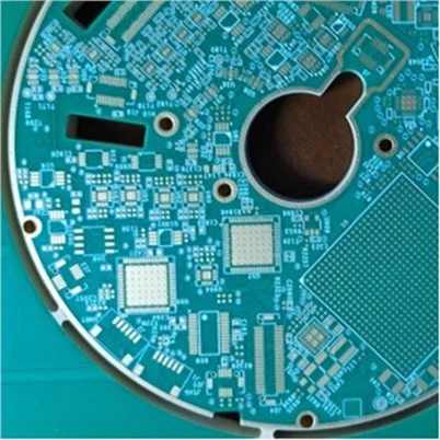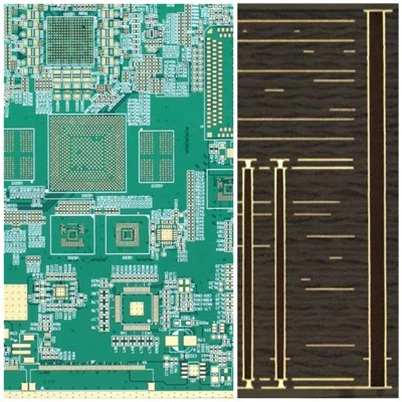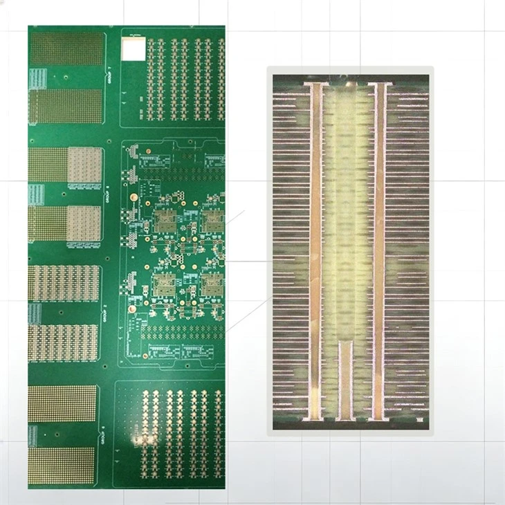
58 Layers Testing Machine Board
This 58-layer ultra-high-layer precision PCB is specially designed for high-end test equipment, with a finished board thickness of 5.5mm. Adopting premium Panasonic M6G high-speed substrate, it is a high-end extreme-process circuit board in the industry. Breaking traditional manufacturing bottlenecks, it achieves an ultra-high board-to-hole aspect ratio of 28:1 and ultra-fine circuit capability of 0.07mm / 0.08mm. The ultra-multi-layer stacked structure supports massive independent signal channel layout, ensuring reliable deep-hole conduction, ultra-dense fine-line routing and excellent dimensional stability. It fully meets the strict requirements of high-precision chip testing, weak signal acquisition and multi-channel synchronous testing, serving as the core carrier mainboard for sophisticated test equipment.
Description


Core Specifications
- Layers: 58 Layers
- Finished Board Thickness: 5.5mm
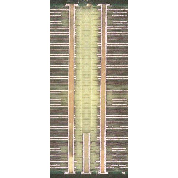
- Board-to-Hole Aspect Ratio: 28:1 ultra-high aspect ratio, realizing reliable electroplating and conduction for micro deep holes on thick boards
- Line Width / Spacing: 0.07mm / 0.08mm ultra-fine circuit, greatly improving wiring density
- Material: Panasonic M6G high-speed substrate with excellent heat resistance, low thermal expansion and stable impedance performance
Core Advantages
- 58-Layer Ultra-high Stack-up, Strong Multi-channel Integration: The 58-layer high-density stack-up reasonably distributes signal layers, power layers and ground layers, supporting hundreds of independent test signal channels without multi-board splicing, which simplifies the internal structure of test equipment. Professional multi-lamination technology effectively controls board warpage and deformation, ensuring high assembly accuracy and stable electrical parameters during long-term continuous testing.
- 28:1 Extreme Aspect Ratio, Zero-defect Deep-hole Conduction: Aiming at the processing difficulties of micro holes on 5.5mm thick boards, it adopts precision deep-hole drilling and uniform thick copper electroplating technology. The hole walls feature complete plating without voids or cracks, ensuring highly consistent via conduction and eliminating test data errors caused by poor contact, so as to guarantee accurate and reliable detection results.
- Ultra-fine 0.07mm Circuit for Dense Microchip Wiring: The ultra-fine 0.07mm line width and 0.08mm line spacing maximize wiring capacity per unit area. It is perfectly suitable for dense layout of micro BGA chips and high-density probe test modules, featuring low weak signal transmission loss and strong anti-interference ability for high-precision micro signal collection scenarios.
- High-stability Panasonic M6G Substrate for Long-term Operation: Panasonic M6G industrial high-speed substrate owns high Tg, low thermal expansion, outstanding moisture resistance and thermal shock resistance. It avoids delamination and bubbling after multiple high-temperature lamination cycles. With consistent impedance and negligible dimensional & electrical fluctuation under temperature cycling conditions, it is highly applicable for long-term repeated power-on testing of precision test equipment.
Application Fields
Chip probe test equipment, semiconductor automatic detection equipment, high-precision signal testing instruments, industrial control precision test mainboards, and laboratory multi-channel test control systems.
Hot Tags: 58 layers testing machine board, China 58 layers testing machine board manufacturers, suppliers, factory, 20 Multi Layer PCB, 20Layer Printed Circuit Board, 24 Multi Layer PCB, Multi Layer PCB, Multi Layer PCB with Blind Hole Board, Multilayer mechanical blind hole board
Send Inquiry
You Might Also Like