Multi Layer PCB with Blind Hole Board
The blind hole is a through hole that connects the surface layer and the inner layer without penetrating the whole plate. Multi-layer circuit board, as the name suggests, is a circuit board with more than two layers can be called multi-layer.
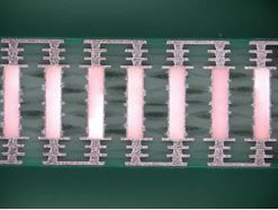
Description
Introducing the Multi Layer PCB with Blind Hole Board
In the world of electronics manufacturing, printed circuit boards (PCBs) are essential components that connect electrical and electronic components in various devices. PCBs are at the heart of electronic devices, making them reliable, efficient, and functional. PCBs have evolved over the years to accommodate new design requirements, such as smaller sizes, higher density, and increased functionality. One such evolution is the Multi Layer PCB with Blind Hole Board, and in this article, we'll introduce this product and highlight its key features and advantages.
The Multi Layer PCB with Blind Hole Board is a type of printed circuit board that has multiple layers of conducting material and insulating material. The conducting material layer is typically made of copper, which is etched to form a circuit pattern. The insulating material in between the conductive layers provides isolation and protection.
Blind holes are drilled holes that go partially through a PCB from one surface to an inner layer, but not through the entire board. Blind holes are used to connect the top and bottom layers of a PCB to the inner layers, without going through the full thickness of the board. The Multi Layer PCB with Blind Hole Board has blind holes that are drilled only on the top or bottom layer and do not penetrate through the entire board, ensuring the secure and efficient transfer of electrical energy.
Key Features of the Multi Layer PCB with Blind Hole Board
High-Density Design
The Multi Layer PCB with Blind Hole Board are designed to provide high-density interconnects, allowing for a large number of connections and circuits to be placed within a small area. This design feature reduces the overall size of the electronic device, making it more compact and lightweight.
Improved Thermal Performance
Multi Layer PCB with Blind Hole Board offers improved thermal performance due to its high-density layer design. With the increased amount of interconnects, heat generated within the PCB can be dissipated at a faster rate. This is important in electronic devices that generate significant amounts of heat, such as power supplies and processing units.
Greater Signal Integrity and Reduction in Signal Loss
The Multi Layer PCB with Blind Hole Board provides greater integrity and consistency for signals passing through the PCB. The high-density design reduces the influence of external electromagnetic interference and minimizes signal loss, resulting in improved signal quality.
Higher Flexibility
The Multi Layer PCB with Blind Hole Board is a flexible design with multiple layers of conductive and insulating materials. This feature allows the PCB to bend and flex without breaking, making it ideal for use in electronic devices that require flexibility and durability.
Cost-Effective
The Multi Layer PCB with Blind Hole Board offers a cost-effective solution for electronic device manufacturers. With its high-density design, multiple connections can be made within a smaller area, allowing for a reduction in the number of interconnects required, thus reducing costs.
Advantages of the Multi Layer PCB with Blind Hole Board
There are several advantages of using the Multi Layer PCB with Blind Hole Board in the manufacture of electronic devices.
1. High-Density Circuit Interconnects
The Multi Layer PCB with Blind Hole Board allows for a larger number of interconnects and circuits to be placed within a small area. This results in a more compact and efficient electronic device.
2. Improved Thermal Performance
The Multi Layer PCB with Blind Hole Board has improved thermal performance, thanks to its high-density design. This makes it ideal for use in electronic devices that generate significant amounts of heat.
3. Better Signal Integrity and Less Signal Loss
The Multi Layer PCB with Blind Hole Board delivers improved signal integrity and less signal loss, resulting in better signal quality.
4. Greater Flexibility
The Multi Layer PCB with Blind Hole Board is a flexible design that can bend and flex without breaking, providing greater flexibility and durability.
5. Cost-Effective
The Multi Layer PCB with Blind Hole Board is a cost-effective solution for electronic device manufacturers, thanks to its high-density design and reduced interconnects required.
Conclusion
The Multi Layer PCB with Blind Hole Board is a high-density design that offers improved thermal performance, better signal integrity, greater flexibility, and is cost-effective. These features and advantages make it an ideal choice for manufacturers of electronic devices. It's essential to partner with a reliable and experienced PCB manufacturer to ensure the best quality and performance of this type of PCB.
The blind hole is a through hole that connects the surface layer and the inner layer without penetrating the whole plate. Multi-layer circuit board, as the name suggests, is a circuit board with more than two layers can be called multi-layer. Multi-layer blind hole circuit board refers to a board with more than two layers and blind holes in the substrate. The blind hole is located on the top and bottom surfaces of the printed circuit board, with a certain depth, and is used to connect the surface line and the inner line below.
In the process of PCB production, blind hole making is the key technology in HDI production, mainly focusing on laser drilling. In the process of laser drilling, it is very important to control the aperture. The main factors affecting the blind hole diameter are wavelength, laser type and diameter, focusing distance, etc. The beam diameter is the key to controlling the aperture.
 |
Item: Multi layer PCB with blind hole board Layer: 20 Board thickness: 2.7mm Key points: blind hole 0.2mm |
Technical Capacity

Why choose us?
- Our in-house capabilities allow us to offer fast turnaround times on Multi Layer PCB orders.
- We have mature equipment, understand the needs of users and products, to ensure that you are satisfied with the Multi Layer PCB with Blind Hole Board.
- Our team is committed to maintaining the highest standards of safety and quality in our Multi Layer PCB manufacturing processes.
- Working with us will save you money and time.
- Our team is comprised of experts who specialize in creating the best Multi Layer PCBs available.
- We actively implement the national industrial policy, seize the opportunity, take the initiative and transform development.
- We work to ensure that our Multi Layer PCB products meet or exceed stringent testing requirements.
- In order to live up to the expectations of stakeholders and realize the optimal sustainable development of society, we take it as our corporate philosophy and actively fulfill our corporate social responsibilities.
- We have a global presence and offer Multi Layer PCB solutions to customers worldwide.
- Our company takes strengthening the reform of production technology as the guarantee, the whole range of market development as the guidance and the continuous enhancement of comprehensive strength to win competitiveness as the development strategy.
Hot Tags: multi layer pcb with blind hole board, China multi layer pcb with blind hole board manufacturers, suppliers, factory, 48 Multi Layer PCB, 48Layer Printed Circuit Board, 80Layer ATE Tester PCB Board, Multi Layer PCB, Multi Layer PCB with Blind Hole Board, Multilayer mechanical blind hole board
Send Inquiry
You Might Also Like