
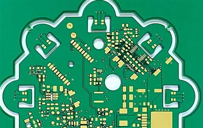
What Is Printed Circuit Board?
A printed circuit board (PCB) is an electronic assembly that uses copper conductors to create electrical connections between components and provide mechanical support for them. PCBs are made of non-conductive material with conductive lines printed or etched into it. Electronic components are then mounted on the board, and the traces connect the components to form a working circuit.
Why Choose Us
Professional Team
A security service provider trusted by customers, it serves customers in many industries such as government and enterprises, finance, medical care, Internet, e-commerce and so on.
Technical Support
Our team of experts is available to assist with troubleshooting, answer technical inquiries, and provide guidance.
Reliable Supply
We offer a vertically integrated supply chain model to ensure reliable long-term supply and complete traceability.
Customer Service
We prioritize open communication to address our clients' specific requirements and deliver personalized solutions.


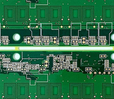


PCBs are made by isolating the surface copper foil conductive layer through the board base insulation material, which allows current to flow through various components along a pre-designed route, ultimately achieving functions such as power making, amplification, attenuation, modulation, demodulation, and coding.
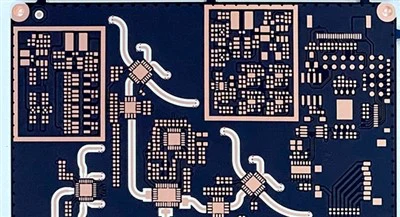
Understanding how a printed circuit board works should start with its composition. The entire PCBA board is composed of bare boards and components, such as microchips, resistors, capacitors and connectors. Manufacturers attach components to the PCB by solder mounting or other techniques. Take, for example, a single-sided PCB, a board that has electronic components and wires on only one side of the board. Usually we mount the components on a non-conductive board by SMT assembly technology or PCBA DIP assembly technology and connect them through small paths called traces. The traces allow the electrical components on the entire board to function by energizing them. Not all hardware devices are directly mounted on the PCB, components such as monitors and cameras are attached to the PCB through mating connectors and flat cables.
The working principle of double-sided and multi-layer circuit boards is to introduce process gas (Ar, N2, O2, etc.) in the high vacuum link, and the gas is ionized into plasma. Under the action of the electric field, these plasmas move toward high potential and low potential respectively. The atomic groups moving toward the low potential bombard the target (copper), so that the copper atoms are stripped from the copper, and finally covered on the substrate (FRP), that is, the copper clad laminate. This is a traditional physical method, which has the advantages of no pollution and mature technology. The disadvantage is that the efficiency is slow and the cycle is long. If you want to quickly realize the PCB manufacturing process, you can lay the etched pattern in advance, and then form the PCB in the above way, and the inner hole for connection can also be plated with metal copper to make it metallized.
Advantages of Printed Circuit Boards
A Compact Solution
A printed circuit board can contain a number of parts and elements. Because they utilize copper tracks rather than actual wires, it allows for the same types of results without using current-carrying wires. The boards are smaller and they are not as bulky. This is one of the reasons that so many different types of electronic devices are smaller than they were in the past. The PCBs have helped to push technology forward in a number of different ways. It's now possible to have highly complicated circuits in very small packages.
Saving Time and Energy
One of the best benefits of using printed circuit boards is the amount of time that can be saved. Connecting components traditionally takes a lot of time, whereas the circuit board will take far less time to assemble once the design is complete. The design phase is often what takes the most amount of time with printed circuit boards, but even this can be reduced when using the right type of software for its creation. AdvancedPCB actually provides customers with a free piece of software called PCB Artist. It is easy and intuitive to use and it provides a relatively simple way to design and test the printed circuit board before moving on to the rest of the process.
No Loose Connections
The connections in the printed circuit board are made through the copy tracks, and as long as they have been manufactured properly, you are not going to have to deal with short circuits or loose connections. Compare this to other methods using actual wires, which could become loose when the board moved. In some cases, the wire itself might have a connection problem. This can all be difficult to trace and to locate the source of the actual problem. With printed circuit boards, these types of issues are nonexistent. If there are problems with the board, it tends to be easy to diagnose and to repair.
A Reliable Option
It's no accident that so many companies and individuals today are making use of printed circuit boards. They are a reliable solution that can work for a wide range of uses and products both large and small. They can last a long time when they have been made properly, which will give people more confidence with the electronics they are using. This is true whether that device might be a phone, a computer, or a military-grade piece of equipment that is used in a less than forgiving environment.
Low Costs
Of course, when it comes to creating and manufacturing various types of electrical goods, the cost is very important. Fortunately, once the circuit board has been designed and tested to ensure that it is working properly, mass production is very affordable. There are fewer components being used in most cases, which helps to reduce the cost to an affordable level for most companies.
Types of Printed Circuit Boards
In general, boards can be categorized into three categories: rigid, flex, or metal-core.
Rigid boards are often the vast majority of boards a designer will encounter, where the layout of the board is contained within a rigid substrate created from a high heat and pressure lamination process. The common material for these boards is FR-4, but depending on the particular needs of the design, this can be modified to emphasize or otherwise improve certain characteristics of the board.
Flexible boards are composed of a less rigid material that allows for far greater deflection. The material is tactilely reminiscent of a film roll, and the board thickness is usually far less than a standard rigid board. While they already see major usage, there is hope that flexible boards will usher in the next step of wearable technology and remove the current planar constraints inherent to rigid board devices.
A metal-core PCB is something of an offshoot of rigid board designs, with an increased ability to dissipate heat throughout the board to protect sensitive circuitry. This style can be an option for high-current designs to prevent thermal wear and failure.
Wherever controlled electromagnetism exists, printed circuit boards form the infrastructure to maintain it. Of course, circuit boards don't just spring out from nothingness–their design and manufacturing are a huge engineering undertaking unto themselves.
The Process of Printed Circuit Board Design


Before a printed circuit board can be built, it must be designed. This is accomplished using PCB circuit board design CAD tools. PCB design is broken into two main categories: schematic capture to create the circuitry connectivity in a diagram and then PCB layout to design the actual physical circuit board.
Develop the Library CAD Parts
The first step is to develop the library CAD parts needed for the design. This will include schematic symbols, simulation models, footprints for PCB layout, and step models for 3D printed circuit board display. Once the libraries are ready, the next step is to create the logical representation of the circuitry on a schematic. CAD tools are used to place the symbols on a schematic sheet and then connect them to form the circuitry.
At the same time, circuit simulation is run to verify that the design will work electrically the way it is intended to. Once these tasks are completed, the schematic tools will send their connectivity data over to the layout tools.
Layout
On the layout side of PCB design, the schematic connectivity is received and processed as nets that connect two or more component pins. With an outline of the intended board shape on the screen, the layout designer will place the component footprints in the correct locations. Once these components are optimally organized, the next step is to connect the nets to the pins by drawing the traces and planes between the pins. The CAD tools will have design rules built into them that prevent the traces of one net from touching another net as well as governing many other widths and spaces needed for a complete design. Once the routing is complete, the design tools are used again to create manufacturing drawings and the output files that the manufacturer will use to build the board.
The design and manufacturing of a circuit board is a step-by-step process: schematic creation and simulation, setting up PCB design grids and DRCs, component placement, PCB routing, power planes, and finally assembling the BOM and building the board.
Structure and Applications of Printed Circuit Board
Many of the important performance characteristics of a PCB are defined in the stack-up or the arrangement of layers in the PCB. The layer stack-up is built with alternating layers of conductive and insulating material, and with alternating layers of core and prepreg (two types of dielectrics used in the layer stack-up). The dielectric and mechanical properties of the core and prepreg will determine reliability and signal/power integrity in the design, and they should be selected carefully when designing for high-reliability applications. For example, military and medical applications need highly reliable designs that might be deployed in harsh environments, and a PCB for a telecom system might require a low-loss PTFE laminate in a small package.
An example of a PCB stack-up is shown below. In this example, the stack-up implements a 4-layer structure with two internal plane layers (L02_GND for ground, and L03_PWR for power). This type of stack-up is appropriate for IoT devices, lightweight embedded systems, and many other designs that use high-speed protocols. The internal plane arrangement helps ensure power integrity while also providing some shielding against external EMI. The internal plane layers also provide a consistent reference for controlled impedance signals. This type of stack-up is typical for many designs and is often a starting point for many modern printed circuit boards.

Common Components of Printed Circuit Boards
Printed circuit boards are made from a variety of PCB materials and electrical components. Common PCB components include:
Resistors
Resistors transmit an electrical current to produce a voltage and dissipate electric power as heat. They come in a range of materials.
Capacitors
The job of a capacitor is to hold an electrical charge within the board and then release it when more power is needed elsewhere in the circuit. Capacitors typically work by collecting opposite charges on two conductive layers that are separated by an insulating material.
Inductors
These are similar to capacitors in that they store energy. However, they are often used to block signals within the PCB, such as interference from another electronic device.
Transistors
A transistor is an amplifier. It's used to switch or control the electronic signals in a board. There are several different versions of transistors available, but the most common is the bipolar transistor.
Transformers
These are used to transfer the electrical energy from one circuit to another via an increase, or decrease, in voltage.
Diodes
A diode allows the electric current to flow in one direction, but not in the other. As a result, diodes are used to stop the electric current from flowing in the wrong direction and damaging the board and the device. The most popular form of diode is the LED (which stands for light-emitting diode).
Sensors
These devices are used to detect changes in environmental conditions and generate an electrical signal that corresponds to the change. This signal is then sent to other components in the circuit board. Sensors convert a physical element such as light motion, air quality, or sound into electrical energy.
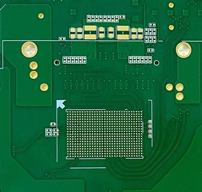
Common PCB layers
Each type of PCB contains a different number of layers that contribute to its functionality. However, no matter which type of PCB you choose, each board contains the same essential foundation. This means that all PCBs contain the following four layers:
Substrate layer
This is usually made from fibreglass, which gives the board its rigidity. Substrate layers can also be made with epoxies, but these lack the durability that fibreglass provides.
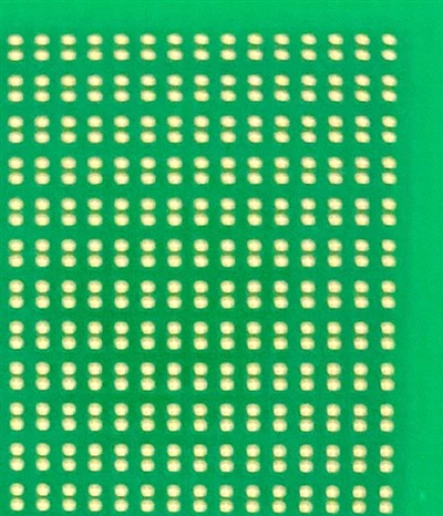
Copper layer
As you'd expect from the name, the copper layer of a PCB is made from a thin layer of copper foil that's laminated to the board using heat.
When we talk about different 'layers' of PCB, we're talking about how many copper layers they consist of. For example, a single sided PCB will only have one layer of conducting material on one side of the board. In this scenario, the other side of the board is used for incorporating different electronic components. Meanwhile, a double sided PCB will mount the conductive copper and components on both sides of the board.
The thickness of the copper layer will be determined by the amount of power the PCB needs to withstand. PCBs that need to handle a higher level of power will have a thicker level of copper.
Solder mask layer
The solder mask layer is placed on top of the copper and provides most PCBs with their green colour. This layer insulates the copper and ensures that it doesn't come into contact with any other elements.
Silkscreen layer
The silkscreen layer is primarily added for the benefit of humans. It involves adding letters, numbers and symbols to the board so it's easier for users to understand the functionality of different pins and LEDs.
Our Factory
Sihui Fuji Electronics Technology Co., Ltd. Founded in 2009, it has been focusing on long-term and reliable circuit board production for 14 years. With the production strength of allegro proofing, mass production, multiple product names, various batches, and short delivery time, it provides one-stop comprehensive services to meet the needs of customers to the greatest extent. It is a chinese electronic circuit board manufacturer with rich experience in quality management of japanese companies. Business.


FAQ
As one of the leading printed circuit board manufacturers and suppliers in China, we warmly welcome you to buy or wholesale bulk printed circuit board for sale here from our factory. All customized products are with high quality and competitive price. Contact us for quotation and free sample.
Metal Half-hole Plate, high-reliability pcb, Correspondence PCB