


16 Layers Back Drilling Pcb
The 16 layer back drilling pcb has a high density. Due to their 16 layers distributed in a small space, they allow chip designers to arrange many electrical circuits and components in a very small space, creating a more compact and highly integrated board. This is crucial for modern mobile...
Description
The 16 layer back drilling pcb has a high density. Due to their 16 layers distributed in a small space, they allow chip designers to arrange many electrical circuits and components in a very small space, creating a more compact and highly integrated board. This is crucial for modern mobile devices and other devices that encounter space limitations.
This board can provide better electrical performance. This is because the circuits on the PCB board are more dense, and their electrical characteristics are destined to be more complex. By balancing these electrical characteristics between several layers of the board, chip designers can achieve better signal transmission and excellent anti-interference performance.
In addition, the board can also bring higher manufacturing efficiency and better reliability. The main reason is that this process can complete more work in a relatively short period of time, while reducing people's manipulation of PCB templates, making it simpler and easier to automate production and manufacturing.
With the increasing use of mobile devices and other small devices, 16 layer back drilling circuit boards will gradually become a more common solution. Its advantages in density, electrical performance, manufacturing efficiency, and reliability will lay a greater market share for it in the future.
The characteristics and advantages of the 16 layer back drilling printed circuit board are obvious. Firstly, it can support more complex circuit designs, thereby adding more electronic components in the same space. Secondly, its energy efficiency is higher than that of a typical 8-layer pcb, with smaller crosstalk effect and wider bandwidth, which means it can better adapt to high-speed transmission and high-frequency applications. Thirdly, the 16-layer back drilling printed circuit board can achieve stricter inter board withstand voltage requirements, prevent wire interference, and thus ensure the stability and reliability of the equipment.
The most critical challenge in the production process of the 16-layer back drilling printed circuit board is the control of the back drilling. The control of back drilling needs to be achieved through plate level control, drilling position accuracy control, and drilling parameter control, striving to achieve high-precision control of drilling direction, spacing, and position while ensuring the height of the back drilling. In addition, due to the increase in the number of layers, the management of foreign objects and stress during the drilling process has become more complex. In order to control the accuracy of back drilling, Sihui Fuji strengthens control from various aspects such as materials, personnel, and equipment, striving to ensure that all production elements are in the best state. We will provide skill training for personnel to provide them with a comprehensive understanding of the characteristics of materials and equipment, as well as the parameters and processing capabilities of the equipment. Regular maintenance and upkeep of equipment to reduce equipment failures and improve equipment productivity.

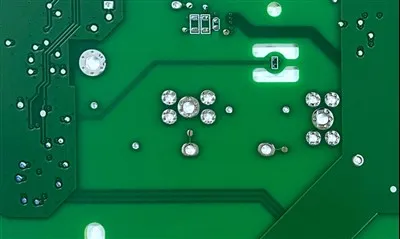
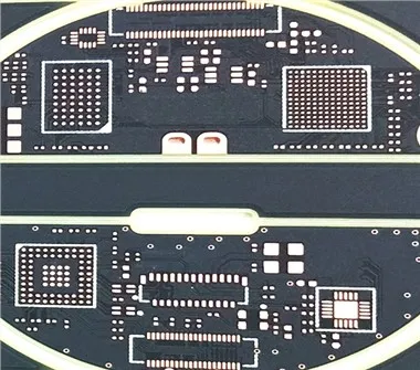
Picture:16 layers back drilling pcb
The 16 layers back drilling pcb has a wide range of applications in the field of communication. After accumulating experience in the production of multiple types of back drilling circuit boards, Sihui Fuji has now gained proficiency in the production technology of this high and multi-layer back drilling substrate, which can achieve mass production and short delivery time.
The specification of sample board
Item:16 layers back drilling pcb
Layer:16
Material:IT-9681TC
Board thickness:2.2±0.22mm
Surface treatment:ENIG
Application field: Communication
Hot Tags: 16 layers back drilling pcb, China 16 layers back drilling pcb manufacturers, suppliers, factory, High Precision Board, Printed Circuit Board, blue Printed Circuit Board, White PCB Board, double layer through hole pcb, Metal Half hole Plate
Send Inquiry
You Might Also Like