Multi-stage Blind Hole Pcb
Multi-stage blind hole pcb is an advanced circuit board technology that can significantly improve the performance and reliability of printed circuit boards. Compared with traditional circuit boards, multi-stage blind hole boards have higher density and finer circuit wiring, enabling more...
Description
Multi-stage blind hole pcb is an advanced circuit board technology that can significantly improve the performance and reliability of printed circuit boards. Compared with traditional circuit boards, multi-stage blind hole boards have higher density and finer circuit wiring, enabling more components and functions to be implemented in a smaller space. At the same time, multi-stage blind hole printed circuit boards also have better electrical performance and impedance control, allowing for more accurate transmission of signals and data.
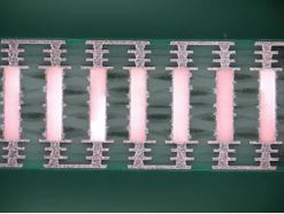
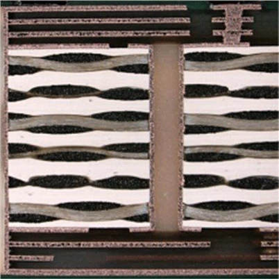
The manufacturing process of multi-stage blind hole circuit boards is relatively complex, requiring high-precision manufacturing processes and equipment. Firstly, it is necessary to lay circuit patterns on the board surface and transfer the patterns to the copper clad layer using photolithography technology. Then, through multiple process steps such as drilling, copper plating, and coating, the circuit board is punched to form a blind hole aperture. Finally, optimize the electrical performance and reliability of blind hole aperture by controlling details such as copper plating thickness and chemical composition of the electrolyte.
The application fields of multi-stage blind hole printed circuit boards are very extensive, including electronic products, communication equipment, medical equipment, aerospace, military and other fields. This technology can significantly improve product performance and reliability, reduce product failure rates and maintenance costs, and also achieve smaller and more efficient product design. Therefore, multi-stage blind hole printed circuit boards will also be increasingly valued and applied in future development.
Compared to traditional PCBs, multi-stage blind hole boards have the following advantages:
1. Multi stage blind hole boards have higher integration, and they can achieve better circuit layout through multi-layer design. Multilayer PCBs allow for more complex circuit diagrams to be arranged in a small space, resulting in smaller PCB designs.
2. The signal transmission of multi-stage blind hole boards is more reliable. For the transmission of high-frequency signals, the blind hole design route is more excellent than traditional circuit boards. Because blind hole design routes can reduce signal reflection and crosstalk, thereby improving the stability and accuracy of signal transmission.
3. The boards can bring better heat dissipation effect. This is because multi-layer PCBs can concentrate heat conduction, resulting in better heat dissipation. Especially for high-power electronic devices, the heat dissipation effect of multi-layer PCBs is very important.
4. The production process of multi-stage blind hole circuit boards is more advanced. Due to the high difficulty in designing multi-layer PCBs, more advanced production processes are needed than traditional PCBs. These processes include laser drilling, blind hole copper sinking, multi-layer stacking, etc. The emergence of these processes has greatly improved the production efficiency and quality of multi-layer PCBs.
Multi-stage blind hole pcb is a very advanced circuit board technology, and its application will greatly improve the performance and reliability of electronic products. I believe that in the near future, multi-stage blind hole printed circuit boards will increasingly become an indispensable part of people's daily lives.

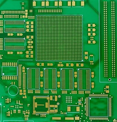
Picture:Multi-stage blind hole pcb
The specification of sample board
Item:Multi-stage blind hole pcb
Material:R-5755G
Layer:12
Board thickness:3.2±0.32mm
Surface treatment:ENIG
Hot Tags: multi-stage blind hole pcb, China multi-stage blind hole pcb manufacturers, suppliers, factory, 10L HDI Board, 4 stage laser via HDI circuit board, 8L HDI circuit board, 16L HDI Board, 3 Stage Laser Via HDI Board, 3 stage laser via HDI pcb
Send Inquiry
You Might Also Like