Five Stages Laser Drilling Pcb
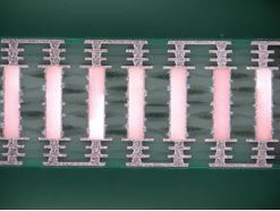
The five stages laser drilling pcb is an 18 layer high multi-layer board. Among them, the dielectric thickness of the board is 200um, and the diameter of laser drilling is 0.20mm, which is produced using the process of laser drilling and resin plugging. The minimum hole copper is 18um, the...
Description
The five stages laser drilling pcb is an 18 layer high multi-layer board. Among them, the dielectric thickness of the board is 200um, and the diameter of laser drilling is 0.20mm, which is produced using the process of laser drilling and resin plugging. The minimum hole copper is 18um, the average hole copper is 20um, and the minimum copper hole drill bit is φ 0.25mm.
With the increasing trend of modern electronic products towards portability, miniaturization, high integration, and high performance, there are more and more micro vias and blind holes between different levels of circuits. Traditional mechanical drilling can no longer meet the requirements of technological development, and has been replaced by laser technology. Laser has characteristics such as high brightness, high directionality, high monochromaticity, and high coherence, bringing unparalleled advantages to laser drilling compared to mechanical drilling.
Laser drilling is non-contact processing, which has no direct impact on the substrate and will not cause mechanical deformation of the substrate. Laser drilling does not use cutting tools in mechanical drilling, and there is no cutting force or other effects on the substrate. Due to the high energy density, fast processing speed, and localized processing of laser beams in laser drilling, it has little or no impact on non laser irradiated areas. Therefore, the heat affected area is small, and the thermal deformation of the substrate is small. Laser beams are easy to guide, focus, and change direction, making them easy to cooperate with CNC systems and process complex substrates. Therefore, they are an extremely flexible processing method. High production efficiency, stable and reliable processing quality.
Of course, laser drilling also has its shortcomings. During the laser drilling process, the most common faults are misalignment of drilling position and incorrect hole shape. The main factors affecting the quality of laser drilling are: materials (including copper foil thickness, resin type, insulation layer thickness, reinforcement material type) and laser system capability (including through hole distribution, through hole spacing, laser wavelength, laser pulse width, and drilling adaptability of different materials).

Picture:Five stages laser drilling pcb
Compared to traditional PCB processing technology, laser drilling printed circuit boards have the following advantages:
High accuracy: Laser drilling printed circuit boards can achieve high-precision drilling and cutting, with aperture accuracy ranging from 0.001 to 0.005 millimeters, and hole spacing and circuit width controlled within 0.02 millimeters. This will greatly improve the electrical performance and reliability of the pcb.
High efficiency: The laser drilling circuit board adopts fully automated production, and the drilling and cutting speed is fast, thereby improving production efficiency and productivity.
Wide applicability: Laser drilling circuit boards can have controllable drilling depth, which can meet the processing needs of various circuit boards, especially suitable for high-density, small aperture, fine circuit and high-frequency circuit board processing.
More Environmental-friendly: the laser drilling printed circuit board does not need to use chemicals and dangerous goods, so it is more environmentally friendly.
The production difficulty of five stages laser drilling pcbs is high, which correspondingly puts higher requirements on circuit board manufacturers. As a printed circuit board manufacturer with 13 years of production experience, Sihui Fuji takes 5S as the starting point, continuously strengthens personnel training and education, purchases new advanced equipment, uses high-quality materials, adopts advanced production methods, and controls various aspects of on-site operations. Efforts are made from all aspects of production to improve product quality and provide customers with reliable and high-quality circuit boards.

Picture:Main Equipment List
The specification of sample board
Item:Five stages laser drilling pcb
Layer:18
Material:TU-883+RO4450F
Board thickness:2±0.2mm
Surface treatment:ENIG
Hot Tags: five stages laser drilling pcb, China five stages laser drilling pcb manufacturers, suppliers, factory, 10L HDI Board, 12 layer circuit board Laser Drilling with blind hole, 14 layer circuit board Laser Drilling, 16L HDI Board, 8 layer circuit board Laser Drilling, 8L HDI pcb
Send Inquiry
You Might Also Like