RF Printed Circuit Board
RF printed circuit board is a type of printed circuit board used for designing and manufacturing wireless communication devices, which can transmit and process high-frequency signals to achieve optimal results. Special processes and materials are used in RF printed circuit boards, such as...
Description
RF printed circuit board is a type of printed circuit board used for designing and manufacturing wireless communication devices, which can transmit and process high-frequency signals to achieve optimal results. Special processes and materials are used in RF printed circuit boards, such as high-frequency organic materials, special circuit layouts, and high-precision manufacturing processes.
RF printed circuit boards are widely used in various wireless communication devices and systems, including mobile phones, satellite communications, radars, satellite navigation, etc. The effectiveness and performance of these devices depend on the quality and performance of the RF printed circuit board.
Like many RF components, PCB materials are classified and compared through many key parameters, including relative dielectric constant (Dk orεr) , dissipation factor (Df), coefficient of thermal expansion (CTE), thermal coefficient constant of Dielectric (TCDk) and thermal conductivity. When classifying different PCB materials, many circuit designers start with Dk. The Dk value of a PCB material refers to the capacitance or energy available between a pair of very close conductors manufactured on the material compared to the same pair of conductors in vacuum.
The biggest characteristic of RF circuit boards is their high-frequency performance. Due to the special skills and materials required for the transmission of high-frequency signals, the materials and manufacturing process of RF printed circuit boards must meet high precision and high requirements.
The Dk value of a PCB material can affect the size, wavelength, and characteristic impedance of the transmission line manufactured on that material. For example, for a given characteristic impedance and wavelength, the size of transmission lines manufactured on PCB materials with high Dk values will be much smaller than that of transmission lines manufactured on PCB materials with low Dk values, although other material parameters may differ. Designers of circuits with loss as a key performance parameter usually tend to use PCB materials with lower Dk values, as these materials have lower losses than materials with higher Dk values.
In fact, PCB materials can lose signal power through four methods: dielectric loss, conductor loss, leakage loss, and radiation loss, although selecting PCB materials can better control dielectric loss and conductor loss. For example, the Df parameter provides a method of comparing the dielectric losses of different materials, where lower Df values represent materials with lower dielectric losses.
For a given transmission line impedance (such as 50Ω), the transmission line on a low Dk material will be physically wider than the transmission line on a high Dk material, and the conductor loss of a wider transmission line will also be smaller. Compared to narrower transmission lines of higher Dk materials, these wider transmission lines can also be converted into higher manufacturing yield (and save production costs). However, the trade-off is that they occupy a larger area on the PCB, which may be a problem for designs that are crucial for miniaturization. The thickness of the PCB substrate, especially its copper conductor layer, also affects the impedance of the transmission line. Thinner dielectric materials and conductors produce narrower conductor widths to maintain the required characteristic impedance.
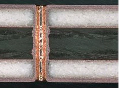
The conductor of PCB material is usually specified by the weight of copper, such as 1 ounce. (35 microns thick) copper or 2 ounces. (Thickness is 70 um) Copper. The quality of these copper conductors also affects conductor losses. Copper conductors with rough surfaces will exhibit higher conductor losses than copper conductors with smooth surface contours.
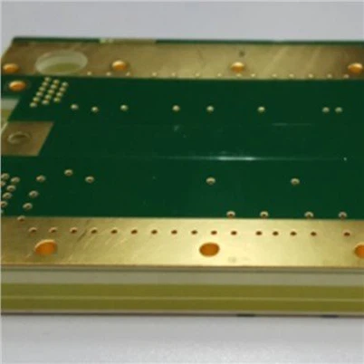
This RF printed circuit board is a circuit board used in 5G products, and Sihui Fuji has successfully trial produced it. If you have any demand for printed circuit boards, please contact us.

Picture:RF printed circuit board
The specification of sample board
Item:RF printed circuit board
Material:RT/DUROID
Layer:2
Board thickness:0.45±0.10mm
Surface treatment:immersion silver
Hot Tags: rf printed circuit board, China rf printed circuit board manufacturers, suppliers, factory, High Frequency Board for 5G Products, High Frequency Board in Electrical Power System, high frequency circuit board for 5G products, high frequency circuit board in electrical power system, high frequency pcb for 5G products, high frequency pcb in electrical power system
Send Inquiry
You Might Also Like