Reasons and Solutions for PCB Blasting
Leave a message
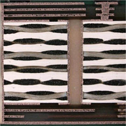
PCB blasting refers to blistering of copper foil, blistering of board, delamination or dip welding, wave soldering, reflow soldering, etc. on finished PCB due to thermal or mechanical action during PCB processing, which refers to the occurrence of Thermal shock. Copper foil blistering, circuit cutting, board blistering, layering, etc. become explosive edges.
Printed circuit board blasting is a key quality issue that affects the reliability of the board, and its reasons are relatively complex and diverse. The main reasons for blistering are manufacturing process issues such as insufficient heat resistance of the board, high working temperature, and long heating time. The reasons are:
1. If the board is not fully cured, the thermal resistance of the board will drop. If the PCB is processed or subjected to thermal shock, the copper clad laminate is easy to blister. The reason for insufficient curing of the board may be due to the low insulation temperature during the bonding process, insufficient insulation time, and insufficient amount of curing agent.
For multi-layer PCB presses, after removing the prepreg from the cold substrate, it must be kept at a temperature of 24 hours in the aforementioned air conditioning environment before cutting and laminating the prepreg onto the inner board. After the lamination is completed, it should be sent to the press for lamination within one hour. This is to prevent moisture absorption of the prepreg, causing white corners, bubbles, delamination, thermal shock, and other phenomena in the laminated products. After stacking and feeding into the press, the air can be released first, and then the press can be closed. This greatly helps to reduce the impact of moisture on the product.
2.If the board is not adequately protected during storage, it will absorb moisture. If it is released during the PCB manufacturing process, the board is prone to cracking. The factories need to repackage unused copper clad boards after opening to reduce moisture absorption on the printed circuit boards.
3.When using copper clad boards with lower TG to manufacture printed circuit boards with higher heat resistance requirements, the low heat resistance of the board can cause the problem of substrate blasting. Insufficient curing of the board can also reduce its TG, which can easily cause the board to burst or turn dark yellow during PCB manufacturing.
In the early production of FR-4 products, only Tg135 ℃ epoxy resin was used. If the manufacturing process is improper, the TG of the substrate is often around 130 ℃. To meet the requirements of PCB users, the Tg of universal epoxy resin can reach 140 ℃. If there are issues with the PCB process or if the board turns dark yellow, high content Tg epoxy resin can be considered.
The above situation is common in composite CEM-1 products. For example, the PCB process of CEM-1 products may experience cracks, and the board may appear dark yellow. This situation is not only related to the heat resistance of the FR-4 adhesive sheet on the surface of CEM-1 product, but also to the heat resistance of the resin composite of the paper core material.
4. If the ink printed on the marking material is thick and placed on the surface in contact with the copper foil, the ink is incompatible with the resin, which reduces the adhesion of the copper foil and makes the substrate prone to deterioration, which may cause blasting.