What is the reason for wave soldering tin connection
Leave a message
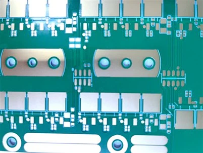
Wave soldering is the process of directly contacting the welding surface of the plug-in board with high-temperature liquid tin, achieving the purpose of welding. The high-temperature liquid tin maintains an inclined surface and forms waves similar to the phenomenon of waves formed by special devices. Therefore, it is called "wave soldering", and its main material is the solder strip.
1. The phenomenon of solder connection caused by the component pins being too long during wave soldering of the printed circuit board. When cutting the component pins for pre processing, please note that the extension length of the component pins is 1.5-2mm, which should not exceed this height. This adverse phenomenon will not occur.
2. Due to the increasingly complex process design of printed circuit boards and the increasingly dense spacing between lead pins, there is a phenomenon of solder bonding after wave soldering. Changing the pad design is the solution. Reducing the size of the solder pad, increasing the length of the solder pad exiting the wave side, increasing the flux activity, and reducing the lead extension length are also solutions.
3. The phenomenon of tin bonding between component pins formed by the infiltration of molten tin onto the surface of the printed circuit board after wave soldering. The main reason for this phenomenon is that the inner diameter of the solder pad is too large, or the outer diameter of the component pins is too small.
4. Wave soldering caused by excessive pad size
5.The phenomenon of solder connection between component pins after wave soldering caused by poor solderability of component pins.
Reason
1. The preheating temperature of the flux is too high or too low, usually between 100-110 degrees Celsius. If the preheating temperature is too low, the flux activity is not high
2. Without the use of soldering flux or insufficient or uneven soldering flux, the surface tension of tin in the molten state is not released, resulting in easy soldering.
3. Insufficient preheating temperature can lead to the inability of the components to reach the temperature. During the welding process, due to the high heat absorption of the components, poor tin dragging can occur, resulting in the formation of tin bonding; It is also possible that the tin furnace temperature is low or the welding speed is too fast.
4.Uneven application of flux
5. Some solder pads or solder legs are severely oxidized
6. There is no solder barrier designed between the solder pads of the printed circuit board, which is connected after being printed with solder paste. Or if the circuit board itself is designed with a solder barrier/bridge, but some or all of it falls off when it is made into a finished product, it is also easy to solder.
7. PCB sinks and deforms during heating, resulting in tin connection.
Solution
1. Control the welding temperature. The welding temperature of the printed circuit board should be appropriate to avoid being too high or too low. If the temperature is too high, the solder is prone to spreading; If the temperature is too low, it may not be possible to fully melt and fix the solder. Therefore, strict temperature control is required during the welding process.
2. Control the welding time. The welding time also needs to be just right. If the time is too long, the solder may spread. If the time is too short, the solder will not cure completely. Therefore, it is necessary to strictly control the welding time.
3. Add shielding. In the manufacturing of boards, some circuits require high-temperature welding, which can easily lead to tin connection problems. In this case, shielding can be added to solve the problem. For example, a metal shield can be covered during the welding process to prevent the solder from spreading to areas that should not be welded.
4. Check the quality of the solder joints. After the welding of the circuit board is completed, it is necessary to carefully check the quality of the solder joints. If there are issues such as solder overflow or weak solder joints, they should be repaired in a timely manner to avoid solder joint problems.