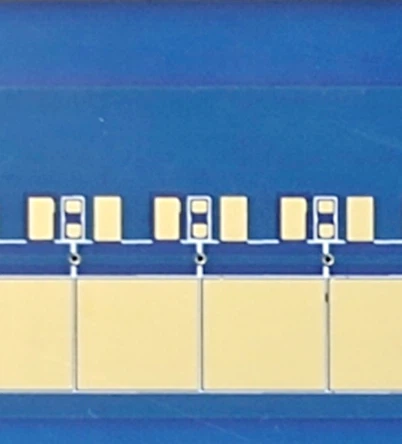
Printed circuit board with pad-in-hole
Leave a message
PCB with pad in hole (PIH) is a new PCB technology that is achieved by drilling holes on the pads in the BGA, QFN, and other packaging areas of the PCB. The advantages of this technology include increasing the density of printed circuit boards, reducing the packaging area, promoting heat transfer, and reducing rebound.
The application of PIH technology was initially in high-speed electronic products, but later gradually expanded to fields such as automotive electronics, avionics, and medical equipment. The biggest difference between PIH and traditional technology is that traditional technology covers a very thin cladding layer on the lower part of the PCB, while PIH drills holes in this layer to vertically import via into the entire pad. One advantage of doing so is that it can reduce rebound and resistance, improve current carrying capacity and conductivity. It can also help optimize the size and shape of printed circuit boards, increase space utilization, and reduce printed circuit board hotspots, providing better assistance for overall system thermal management.
The application of PIH technology has proven its reliability and stability in many different backplane packaging processes. Although this process often requires higher equipment costs and longer production time, it provides better performance and reliability assurance, which is crucial for some high-end products.
PIH technology has provided significant room for improvement in the performance and reliability of electronic devices, and has become a technology that cannot be ignored in the PCB manufacturing industry. It is expected that PIH technology will continue to play an important role in the future electronic and electrical industries, and provide consumers and manufacturers with long-lasting and stable performance and services.