Multi-stage Back Drilling Pcb
Multi-stage back drilling pcb is a high-level printed circuit board (PCB) that is particularly suitable for high-speed data transmission and high-frequency signal processing applications. Compared to traditional double-sided and four-layer boards, multi-stage back drilling printed circuit boards...
Description
Multi-stage back drilling pcb is a high-level printed circuit board (PCB) that is particularly suitable for high-speed data transmission and high-frequency signal processing applications. Compared to traditional double-sided and four-layer boards, multi-stage back drilling printed circuit boards can achieve higher signal quality and smaller board thickness, while shortening the signal transmission path, reducing impedance mismatch and signal cross interference, thereby improving the performance and reliability of the entire system.
The manufacturing process of multi-stage back drilling printed circuit boards is relatively complex and requires multiple steps. Firstly, drill holes between multiple boards on the same layer, and then use depth-controlled drilling technology to process electrical holes on the back. After completion, follow the steps of coating copper foil on the surface of the PCB, processing internal electronic circuits, and finally conducting processes such as gold plating, silk screen printing, and electrical testing.
The multi-stage back drilling pcb has three main advantages
1. Improve signal transmission quality: A multi-layer structure can effectively reduce the impact of signal scrambling and crosstalk, and improve the transmission quality and stability of the signal.
2. Simplify system layout: Multi-stage back drilling printed circuit boards can reduce noise, and isolate complex circuit layouts, thereby achieving the effect of optimizing system layout.
3. Improving signal transmission speed: The biggest advantage of multi-stage back drilling printed circuit boards is that they can reduce the length of the path on the board, effectively reduce signal delay and loss, and improve signal transmission speed.
4.High density electrical performance and reliability: The interconnection of multiple circuit layers allows the board to accommodate more components and connections. The design between different layers can also optimize the circuit layout, reducing the size and volume of the printed circuit board. In addition, through complete metallization treatment, the back drilling can improve the reliability and anti-interference performance of the entire circuit board, making it more suitable for high demand applications.
The production cost of multi-stage back drilling boards is relatively high, mainly due to the need to use more advanced manufacturing technology and equipment. For example, when making multi-layer circuits, it is necessary to first create multiple single-layer printed circuit boards, and then use back drilling technology to connect them together. This involves a large number of manual operations and the use of high-precision equipment, resulting in relatively high production costs.
In terms of technology, the production of multi-stage back drilling printed circuit boards requires mastering some professional technical points. Firstly, it is necessary to be proficient in the design and layout of printed circuit boards, especially when designing in multi-layer circuits, which requires higher circuit design skills.
Secondly, the production of multi-stage back drilling boards involves some advanced process technologies, such as back drilling technology, which requires relevant practical experience and professional knowledge. In addition, in order to ensure the quality and performance of the printed circuit board, it is necessary to conduct strict inspection and testing on the printed circuit board.
Multi-stage back drilling pcb is widely applicable in various fields, including communication devices, embedded systems, servers, network devices, high-speed trains, and autonomous vehicles. In the future, multi-stage back drilling printed circuit boards will play a more important role in the national strategy of next-generation high-speed data transmission and digitization, and will become one of the important means for high-performance and high reliability design of electronic equipment.

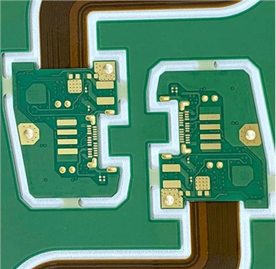
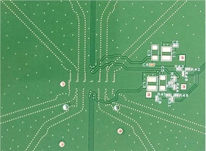
Picture:Multi-stage back drilling pcb
The specification of sample board
Item:Multi-stage back drilling pcb
Material:H175HFZ
Layer:8
Board thickness:0.8±0.18mm
Surface treatment:Immersion silver
Hot Tags: multi-stage back drilling pcb, China multi-stage back drilling pcb manufacturers, suppliers, factory, Metal Half-hole Plate, yellow Printed Circuit Board, Medical pcb, Single layer through hole pcb, white Printed Circuit Board, red Printed Circuit Board
Send Inquiry
You Might Also Like