The introduction of HDI laser drilling
Leave a message
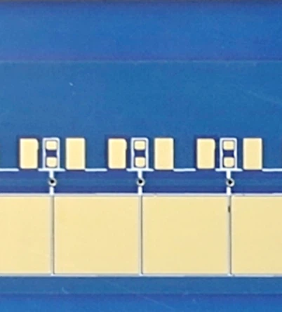
HDI laser drilling technology is a technology of drilling holes in printed circuit boards (PCBs), also known as high-density integration (HDI) technology. It is specially designed for high-end PCBs. It accelerates the whole design process with smaller aperture and shorter cycle time.
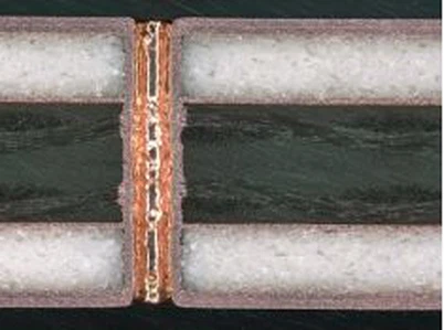
HDI laser drilling helps to improve the integration of PCB circuits, improve their functions, reduce the overall dimensions and broaden the application range. HDI technology uses hydrocarbon laser or waveguide laser to drill holes. It uses a complex process called light infiltration technology to transform the hollow fiber plastic pipe acted by the laser into a solid column.
Then, it uses high-speed airflow to take away the waste column dissolved by the laser. In the light infiltration technology, the diameter range of the hole is very wide, from a few microns to millimeters, and the material produced is durable, heat resistant and not easy to deform. In addition, due to the use of lasers, HDI technology has greatly reduced environmental pollution.
HDI technology has been applied more and more widely. At present, it has been flexibly applied to various scalable electronic designs, such as microcontrollers, highly integrated processors, semiconductor converters, wireless communication systems and other electronic applications.