Considerations and Methods of High Speed and High Density PCB Circuit Design
Leave a message
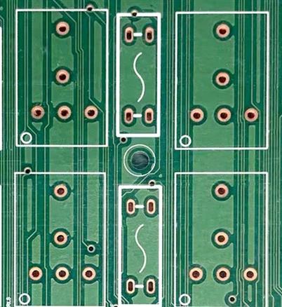
When the size of the circuit board is fixed, if the design needs to accommodate more functions, it is often necessary to improve the wiring density of the PCB. However, this may lead to increased mutual interference of the routing, and the impedance will not be reduced if the routing is too thin. What are the points to be noted and solutions to be taken in PCB design?
When designing high-speed and high-density PCBs, we should pay special attention to crosstalk interference because it has a great impact on timing and signal integrity.
The following points should be noted: control the continuity and matching of the characteristic impedance of the routing. The size of the wire spacing.
It is usually seen that the spacing is twice the line width. Through simulation, we can know the impact of routing spacing on timing and signal integrity, and find the minimum tolerable spacing. Different chip signals may have different results.
Select the appropriate termination method. Avoid that the routing directions of the two adjacent layers are the same, or even that the two layers overlap, because the crosstalk interference is greater than that of the adjacent layers.
Use blind/buried via to increase wiring area. However, the production cost of PCB will increase. It is really difficult to achieve full parallelism and equal length in actual implementation, but we should try our best to do so. In addition, differential termination and common mode termination can be reserved to mitigate the impact on timing and signal integrity.