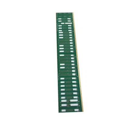
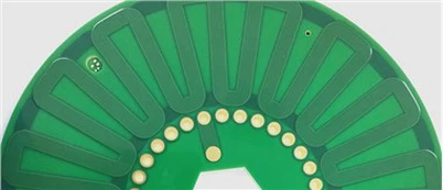
The developing process of printed circuit board
Leave a message
The developing is a technique based on chemical reactions used to make printed circuit board (PCB). In the process of making the printed circuit board, the circuit pattern is designed and laid out first, then the optical resistance is covered on the copper foil, and the desired circuit pattern is etched in the copper foil through the process of exposure and developingt.
The principle of printed circuit board developing is to use chemicals in the developing solution to corrode the exposed copper layer on the surface of the board, enabling the pattern to be presented. The most commonly used developer is an alkaline chloro-ferric solution, whose chemical equation is:
Cu + 2FeCl3 + 2NaOH → Cu(OH)2↓+ 2NaCl + 2Fe(OH)3↓
During the developing process, the developer reacts with the copper layer to produce hydrogen gas and copper chloride ions. Hydrogen gas is released, and copper chloride ions are reduced to copper hydroxide. These chemical changes ultimately result in the depletion of oxygen in the developing solution and the development process ending.
During development, the exposed areas of the front photoresist will solidify and the unexposed areas will dissolve away. Therefore, a chemical developer is needed to help strip the unexposed photoresistance away, leaving only the desired circuit pattern.
There are two types of developers commonly used for printed circuit boards:
1. Alkaline developer: the main component is sodium hydroxide, used to eliminate unexposed photoresistance. But this developer needs to use pure water cleaning, in the process of use need to pay attention to the PH value, otherwise it will affect the quality of the printed circuit board.
2. Acid developer: Acid developer is mainly composed of sulfuric acid, hydrogen peroxide and other components, which can quickly dissolve unexposed photoresistance. But the use of acid developers need to be safe, because sulfuric acid is very corrosive, must be done in a professional laboratory or chemical laboratory.
Note:
1. Developer solution should be stored in a cool, dry, ventilated place, and should be away from fire sources and direct sunlight.
2. Equip yourself with personal protective equipment such as protective gloves, goggles, and a breathing mask.
3. Check whether the container is intact before use to avoid leakage.
4. It should be mixed according to the proportion of the guide and thoroughly stirred before use.
5. Attention should be paid to temperature and time in the development process.
The developer is evenly coated on the surface of the printed circuit board by soaking, spraying, brushing, etc. The length of time the developer stays on the printed circuit board is then adjusted according to the thickness requirements. As the development time increases, the light resistance of uncured exposure is less and less, and the circuit pattern on the board is more and more obvious.
Finally, the developer used in the development process should be thoroughly rinsed and the board surface should be dried with a quick drying solvent. Through the development step, clearly visible electronic component connecting board and printed circuit board can be made.
In the manufacturing of the printed circuit board, there will be unclean development, at this time we should consider from the following aspects:
1. Prebake at too high a temperature or for too long
2. The exposure energy is too high and the vacuum degree is not enough
3. Insufficient film resistance
4. Improper development parameters
5. Dust-free room temperature and humidity
6. Residence time from text screen printing to pre-baking of the circuit board