For the E-tester needle mark of pcb
Leave a message
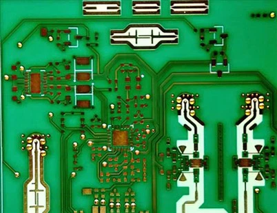
In the process of PCB board manufacturing, in order to ensure that the overall quality meets the requirements, it is necessary to test the performance of electrical parameters and timely find abnormal problems such as short-circuit resistance. Effectively improve PCB production yield, reduce unnecessary losses. Electrical test is to test the current and voltage of the electronic components connected to the circuit board to detect whether the working state of the board is normal. If the clamping speed of the fixture is too high, the speed of the flying needle probe is too fast, and the pressure is too large, the test needle marks will be left on the PCB board.
Needle mark problem refers to the problem where the test needle will cause marks on the surface of the copper plate during pcb electrical test. This will cause changes in the surface capacitance of the copper board, thereby affecting the accuracy of the printed circuit board electrical test. Although needle mark problems often occur in pcb electrical testing, we can actually avoid them through some methods.

At present, the most common surface treatment methods for PCB boards include HASL and gold plating. Different treatment methods are affected by different material, and their ability to withstand electrical parameter performance tests is also different. PCB electrical performance testing includes needle bed testing and flying needle testing. During the testing process, the performance of the printed circuit board was affected. The needle mark treatment is directly related to the surface treatment of other test point. The maximum width of the needle mark on the HASL board should be less than 70um. The factors that affect needle marks include probe structure, material, and control method.
During the electrical test process, it is necessary to automatically control relevant parameters such as needle lift height, stepper motor, subdivision parameters, and starting speed. The test triggered a deceleration action on the micro pressure sensor of the probe mechanism, but due to the influence of the pressure sensor, the process was uncontrollable during the probe test, resulting in various serious needle mark defects that could not meet industry testing requirements. This conventional test probe motion control method cannot achieve good control. At present, a more advanced control method can install a laser sensor on the test probe to ensure reasonable control of needle marks.

In order to effectively detect the problem of needle marks generated during the flying probe test process, we can reproduce the phenomenon and ultimately determine the process of scratch generation. At the same time, we can also control the probe speed, movement speed, and depth of the welding pad furnace barrel of the flying probe. The scratches are affected by the continuous needle flying problem, concentrated in the plug area, resulting in a relatively high density of measuring points in the row of sockets. The root causes of needle marks are board thickness, needle lift height, and probe movement speed. It is necessary to repeatedly consider the comprehensive factors of the lifting height and movement speed behind the board to effectively solve the problem of needle marks.
At present, flying probe test includes knife shaped needles, needle shaped needles, and low resistance needles, with different types of needles producing different needle marks under the same conditions.
Solving the electrical test needle marks on printed circuit boards requires a complex process that takes into account multiple factors. By taking appropriate preventive measures, we can improve the quality and performance of printed circuit boards while maintaining production efficiency and reliability.