Design of PCB panelization
Leave a message
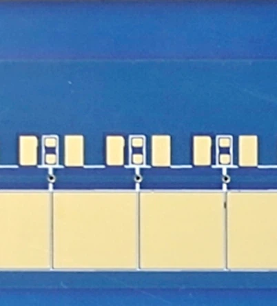
A 1.6mm or 2.4mm space shall be reserved between each unit board of PCB in the panel to facilitate the division of gongs or punches. On the four corners of the panel, NPTH shall be designed. The entire panel shall ensure at least two holes, and the hole size is 3.05 ± 0.05mm. The center of the hole should be positioned at the corner of the circuit board, 5mm in X and Y directions respectively. The four corners of the panels should be designed with 5mm radius R corner to prevent clamping on the track conveyor belt.
The panel design must ensure that the distance between the edge of the reference point and the panel edge is at least 5mm. The reference points on both sides should not be placed symmetrically, which can prevent PCB from entering the machine in reverse through the identification function of the device itself. A direction sign can be designed at the edge of the panel to prevent PCB from being in the wrong direction during production. The maximum profiling tolerance of the panel shall be controlled within 0.05mm.
If PCB manufacturers want to design a good panelization drawing, they must have sufficient information support, otherwise, the quality problems of subsequent SMT assembly or division may be caused due to unreasonable panel design. To complete a qualified panel design, the following data information is usually required. The Gerber data, which contains the component distribution, considers the partition spacing and the placement of connection points. Profiling drawing, understand the overall dimensions and specifications. The specification of large components, especially plate edge components, requires the design of panel spacing, avoidance, etc.
In any case, PCB assembly is designed to meet the assembly requirements and safe operation of SMT. After assembly, it is still necessary to return to the assembly of finished boards. Therefore, regardless of hard boards or soft boards, both the assembly strength requirements and the board splitting requirements after production should be considered in the design of PCB assembly.