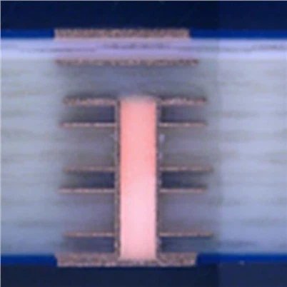
Advantages of ceramic substrates
Leave a message
◆The thermal expansion coefficient of the ceramic substrate is close to that of the silicon chip, which can save the Mo chip of the transition layer, save labor, material and cost;
◆Reduce solder layer, reduce thermal resistance, reduce voids, and improve yield;
◆Under the same current carrying capacity, the line width of 0.3mm thick copper foil is only 10% of that of ordinary printed circuit boards;
◆ Excellent thermal conductivity makes the package of the chip very compact, so that the power density is greatly improved, and the reliability of the system and device is improved;
◆ Ultra-thin (0.25mm) ceramic substrate can replace BeO, no environmental toxicity problem;
◆Large current carrying capacity, 100A current continuously passes through the 1mm wide 0.3mm thick copper body, the temperature rise is about 17℃; 100A current continuously passes through the 2mm wide 0.3mm thick copper body, the temperature rise is only about 5℃;
◆Low thermal resistance, the thermal resistance of 10×10mm ceramic substrate is 0.31K/W with a thickness of 0.63mm, the thermal resistance of a 0.38mm thick ceramic substrate is 0.19K/W, and the thermal resistance of a 0.25mm thick ceramic substrate is 0.19K/W. Thermal resistance is 0.14K/W.
◆ High insulation withstand voltage to ensure personal safety and equipment protection.
◆ New packaging and assembly methods can be realized, making the product highly integrated and compact.