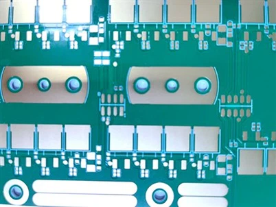
About the Panelization of printed Circuit Board
Leave a message
Panelization of pcb is the combination and splicing of multiple small-sized printed circuit boards to form a large-sized pcb.
The purpose of panelization is, firstly, to facilitate customers' soldering and mounting of printed circuit boards. The second is that pcb manufacturers can reduce waste and save costs during the production process.
The method of panelization
1.Add break away tab on board edge, no spacing
This method is suitable for customers who do not have special requirements for appearance or burrs. We can directly break along the V-cut line, but there may be slight burrs around the board, which generally does not affect the actual installation and use of customers, and such board edges are also easy to polish. In addition, the addition of process edge stitching enhances the strength of the stitching and makes it more resilient during placement. This splicing method with process edges can fix the substrate in the subsequent production process, making it easy to process.
2.Add break away tab on board edge with spacing
If the customer has particularly high requirements for the outer line of the printed circuit board, and the board edges cannot have burrs, they need to mill the board edges. This way, there needs to be space between the boards, usually 1.5-2mm, which is conducive to controlling burrs. In addition, the size of the board is too small to pass through the V-cutting machine, and spacing needs to be set.
3.No break away tab
Some products require manual assembly and can be made without break away tab, as long as there are positioning holes inside the board. This type of assembly can save the cost of board edges and appropriately reduce the production cost of printed circuit boards.
There are many ways to connect printed circuit boards, with two common ones being V-cut and stamp holes.
V-cut has the advantages of low cost, easy separation of boards, and neat edges after separation. The production method is to assemble multiple PCB boards together and cut a V-shaped groove at the connection between the boards, making it easy to separate. Due to the fact that V-cut can only be cut into straight lines and cannot change direction, it is more suitable for rectangular PCB boards. The V-cut splicing method has certain requirements for the thickness of the PCB, generally requiring a board thickness of more than 1mm. If the PCB board is too thin and V-cut is used, it will damage the original strength of the board.
Stamp holes are another way of connecting boards by drilling small holes at the joints of the boards to form a connecting strip. The size of the stamp hole is generally around 0.3mm, and the spacing between the holes is generally around 1mm, making it easy to break and split the board. Because the broken edge presents a jagged shape similar to the stamp edge, it is called a stamp hole.
Due to the decreasing volume of PCBs and their inability to meet the requirements of fixtures, it can lead to low production efficiency. And if the PCB with irregular shape is produced on a single chip, it will also cause a large amount of substrate waste, and splicing processing can effectively solve these problems.
The main advantage of printed circuit board panelization is that it can improve production efficiency. Compared to directly producing large printed circuit boards, the production process of assembling multiple small circuit boards is simpler, and the production of multiple small printed circuit boards can be carried out in parallel. In addition, pcb panelization can also reduce production costs. Due to the short production cycle and low cost of small printed circuit boards, assembling multiple small printed circuit boards can avoid the high cost and low efficiency issues of producing large printed circuit boards.
The disadvantage of pcb panelization is that it is prone to problems such as circuit misalignment and different processes during the assembly process. These issues may lead to a decrease in product quality and production efficiency. Meanwhile, due to the need to assemble multiple small printed circuit boards together, the panelized parts are usually relatively thick and heavy, which may affect the overall performance of the product.